Thermal Camera Inspires Your PCB Inspection and Repair Efficiency
In the world of electronics, the rapid advancement of technology has led to the development of complex and intricate Printed Circuit Boards (PCBs). Ensuring the functionality and reliability of these PCBs is crucial, making the inspection and repair processes essential in various industries. One technology that has revolutionized the way PCBs are inspected and repaired is thermal imaging cameras. This blog explores how thermal cameras have become a game-changer, boosting efficiency in PCB inspection and repair processes.
Understanding Thermal Cameras
Thermal cameras, also known as infrared cameras, are devices that capture the heat signatures emitted by objects. Unlike traditional cameras that capture visible light, thermal cameras detect the infrared radiation produced by varying temperatures. This technology enables the visualization of temperature differences, helping to identify anomalies that could indicate defects or malfunctions within electronic components.

The Challenges in PCB Inspection and Repair
Modern PCBs are densely packed with miniature components, making manual inspection and diagnosis increasingly challenging. Identifying hidden defects such as cold solder joints, overheating components, or poor connections demands precision. Traditional methods like visual inspection and electrical testing may fall short when it comes to diagnosing subtle temperature-related issues. Here's where thermal cameras come into play.

Role of Thermal Cameras in PCB Inspection
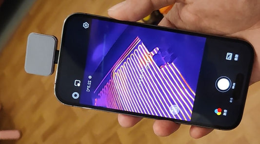
Thermal cameras provide a non-contact and non-invasive way to measure the temperature of various components on a PCB. By capturing thermal images, these cameras identify hotspots and temperature variations that can signal potential defects. Hotspots might indicate excessive resistance, faulty components, or inadequate cooling, while cold spots could point to poor connections or malfunctioning parts.

Integrating Thermal Imaging in the Repair Process
The introduction of thermal cameras in the repair process enhances the accuracy and speed of diagnosis. Technicians can use thermal data to pinpoint the exact location of defects, reducing the time spent on trial and error. By identifying the root cause of the issue quickly, repair strategies become more targeted and effective. This translates to less downtime and lower costs associated with unnecessary component replacements.
Advancements in Thermal Imaging Technology
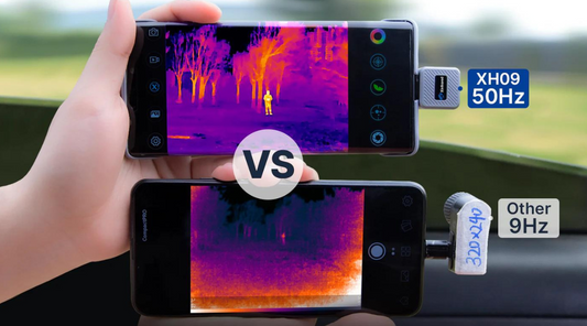
Recent advancements in thermal imaging technology have further propelled its effectiveness. Higher resolution and sensitivity enable the detection of even smaller temperature variations, allowing for more precise defect identification. Furthermore, automation and AI-assisted analysis streamline the interpretation of thermal data, expediting decision-making.
Training and Skill Development
While thermal cameras offer powerful capabilities, their effective use requires proper training. Technicians need to understand how to interpret thermal patterns accurately and differentiate between benign temperature variations and actual defects. Integrating thermal imaging into existing inspection protocols necessitates training programs that cover camera operation, image analysis, and troubleshooting.

Limitations and Considerations
It's essential to acknowledge the limitations of thermal imaging technology. Surface defects are more readily detectable than internal ones, which might require additional methods. Different components also exhibit varying thermal characteristics, making it necessary to establish baseline temperature values for accurate analysis. Additionally, factors such as ambient temperature and electromagnetic interference can affect thermal readings.
In the realm of PCB inspection and repair, efficiency is paramount. Thermal cameras have emerged as a groundbreaking tool that enhances these processes by offering a non-invasive, real-time view of temperature variations. By swiftly identifying defects and anomalies, technicians can make informed decisions, reducing downtime, and minimizing costs. As technology continues to evolve, the integration of thermal imaging into PCB maintenance protocols will likely become an industry standard, ensuring the continued reliability and functionality of electronic devices.


